Sand to Superintelligence: A Beginner’s Guide to the Silicon Stack
How a chip actually gets made, why two companies can stop the entire AI industry, and why AI is both the cause of the bottleneck and the best hope of fixing it.

My first microprocessor
27 years ago at Purdue, in ECE 362, I programmed my first chip: a Motorola 68HC12 with a few KBs of memory, hand-written assembly, bolted onto a racecar so we could control its speed remotely. I still remember the rush. Today the chips driving the AI boom cram 200+ billion transistors into one package, and half the world’s governments are fighting over them. Same starting material: sand. And that distance is what this post is about.
The strange loop at the center of this
Marinate on this for a second:
the technology currently breaking the chip industry is the same technology most likely to fix it.
AI eats chips faster than the world can make them. A single frontier model trains on tens of thousands of leading-edge GPUs. And AI is also the best tool we’ve ever had for designing chips, checking them, and squeezing more of them out of the factories we already have. That tension runs through everything below.
To see why, you have to know how a chip gets made. Most people don’t, and that’s fine; the industry hides behind acronyms. The structure underneath fits on a napkin. So that’s what we drew.
(This post is a companion to our full interactive map at canonical.cc/labs/semiconductor-silicon-stack, which tracks 20 incumbents and 40+ challengers across every layer)
The stack, on a napkin
A chip starts as quartz sand and ends as a die with billions of transistors. In between: six physical steps, plus one software pipeline running alongside. Each step is dominated by one or two companies you’ve probably never heard of.
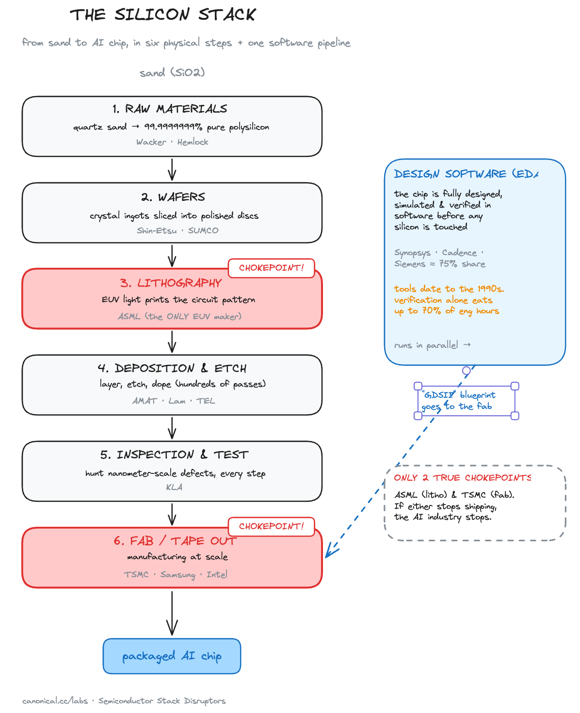
Follow the sand.
1. Raw materials. First you purify sand into polysilicon that is 99.9999999% pure. Nine nines. Take a billion atoms; only one is allowed to be the wrong kind. Two companies, Wacker and Hemlock, dominate, not because the chemistry is secret but because nobody else wants to run a billion-dollar chemical plant that needs a decade of contracts to pay for itself.
2. Wafers. The polysilicon gets grown into a single perfect crystal, then sliced into mirror-polished discs. Two Japanese companies, Shin-Etsu and SUMCO, make most of the world’s supply.
3. Lithography. The famous one. You print the circuit pattern onto the wafer with light, and the features are so small that ordinary light is too fat to draw them. So the machine makes its own: it fires a laser at droplets of molten tin, 50,000x/second, and collects the extreme ultraviolet flash with mirrors so smooth that if you stretched one to the size of a country, the tallest bump would be about a millimeter. One company on Earth makes these machines: ASML, in the Netherlands. The newest model runs $380 million. There is no second source. None.
4. Deposition and etch. Now you build the chip up like a layer cake, hundreds of layers, depositing material and etching it away. Applied Materials, Lam Research, and Tokyo Electron split this market. A healthy three-horse race, though each horse specializes in different tools.
5. Inspection and test. After every step, you hunt for defects a few nanometers wide. Miss one and the chip is garbage. KLA owns this.
6. The fab. TSMC in Taiwan puts the whole symphony together at scale. Samsung is a credible second on some nodes. Intel is rebuilding. At the true leading edge, though? TSMC or nothing.
And running alongside all of it: design software, called EDA. Before anyone touches silicon, the chip lives entirely in software, where it’s designed, simulated, and torture-tested. Three companies (Synopsys, Cadence, Siemens) hold about 75% of that market, with tools whose bones date to the 1990s.
Notice who’s missing: Nvidia. It doesn’t make chips. Neither do AMD or Apple. They’re “fabless”: they design in the EDA tools and hand TSMC the blueprint. The companies above are the ones even trillion-dollar giants depend on.
So where does it break?
Now ask the question a curious person should ask: which of these layers could actually stop the world?
Only two. ASML and TSMC.
If either one stops shipping, the AI industry grinds to a halt within months. Every other layer has at least two serious competitors keeping each other roughly honest.
“Semiconductor shortage” is a vague phrase hiding a precise reality. The world isn’t short on sand, wafers, or etch tools. It’s short on EUV exposures and leading-edge fab slots, which funnel through exactly one Dutch company and one Taiwanese one. And TSMC’s grip goes beyond printing silicon: the advanced packaging that stitches finished dies into a working accelerator also runs mostly through it. Hold that thought.
Where AI causes the squeeze
Now pour the AI boom into that structure and watch where it pinches.
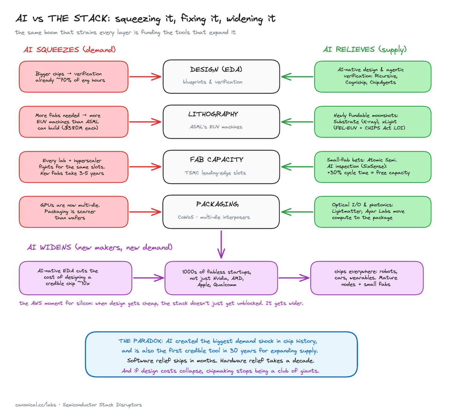
The fab layer takes the direct hit. Everyone who matters (hyperscalers, frontier labs, now entire countries) is fighting over the same TSMC capacity. And you can’t panic-build a fab. Demand moves in months. Fabs move in half-decades and cost tens of billions.
The pressure flows downhill to lithography. More fabs means more EUV machines, and ASML can only assemble so many a year. Each machine has hundreds of thousands of parts, from a supply chain that is itself backed up.
Meanwhile the design side has its own problem: people. AI chips are enormous, and verification, the work of proving a design is correct before you bet $100M+ on manufacturing it, already eats up to 70% of engineering hours on a project. You can’t hire your way out. Training a chip designer takes a decade.
And the chips themselves changed shape. A modern AI accelerator isn’t really one chip. It’s several dies stitched together on an interposer (that’s the CoWoS packaging you’ve maybe heard of), and that stitching capacity is scarcer than wafers.
The pain shows up exactly where competition is thinnest. Not a coincidence.
Where AI relieves it
Here’s the other half of the loop, and the part I find more fun.
On the software side: the people behind Google’s AlphaChip, which used reinforcement learning to lay out chips better than human engineers, left to start Ricursive Intelligence. Salt the claims in this category appropriately. But the direction matters: if AI compresses design cycles from years to months, every design team on Earth just got bigger overnight.
On the hardware side, AI money is funding swings at the chokepoints themselves, which nobody dared for decades. Substrate aims to make chip-printing light with particle accelerators instead of ASML’s tin droplets.
Those are 2 of many. Agentic verification copilots, AI inspection layers squeezing 30% more throughput from existing fabs, free-electron-laser EUV with CHIPS Act backing: the full roster, with traction numbers and caveats, lives on the map.
Will any of them dethrone ASML or TSMC this decade? Almost certainly not. Watch the software layer instead: software ships in months, and the incumbents’ AI offerings are bolt-ons, not rebuilds.
Why hasn’t a 30-year-old monopoly been disrupted already? Rational fear. When a manufacturing run costs $100M+, nobody volunteers to be first to trust an unproven tool. That’s the real moat: challengers can’t just be better, they have to be provably, boringly, run-after-run better.
But if AI draws blood anywhere first, it will be EDA.
The part that should excite you
Follow that thread one more step and you get to the prediction I’d actually bet on. Today, designing a serious chip costs so much (tens of millions in tools and talent before you even pay for manufacturing) that custom silicon is a rich company’s game. “Fabless” mostly means Nvidia, AMD, Apple, Qualcomm.
We’ve seen what happens when that kind of cost collapses. Renting a server from AWS turned “starting a software company” from a $5M proposition into a weekend project, and we got millions of software companies. If AI-native design tools cut the cost of a credible chip by 10x, you don’t get slightly more chip companies. You get thousands of fabless startups designing silicon for problems too small for Nvidia to bother with.
And the demand is already lining up. Physical AI is pushing intelligence into robots, cars, drones, wearables, and factory floors, and most of those chips don’t need the bleeding edge. They need to be cheap, low-power, and exactly right for one job. (We map that whole demand wave separately on our Physical AI & Robotics tracker)
A world of thousands of designs running on mature nodes is also the world where Atomic Semi’s many-small-fabs bet stops sounding crazy. More designers, more specialized chips, more places to make them.
Somewhere on a campus right now, a junior is flashing their first assembly program onto a microcontroller and feeling the same rush I felt with that racecar. The stack they inherit is being rebuilt today.
The hardware chokepoints are decade-long bets you underwrite like fusion. We track all of it, layer by layer, with sourcing and known caveats, on the full interactive map: Semiconductor Stack Disruptors
Educational, not investment advice. Data is point-in-time as of May 2026.