The Memory Wall: Where AI’s Second-Order Effects Hit Silicon

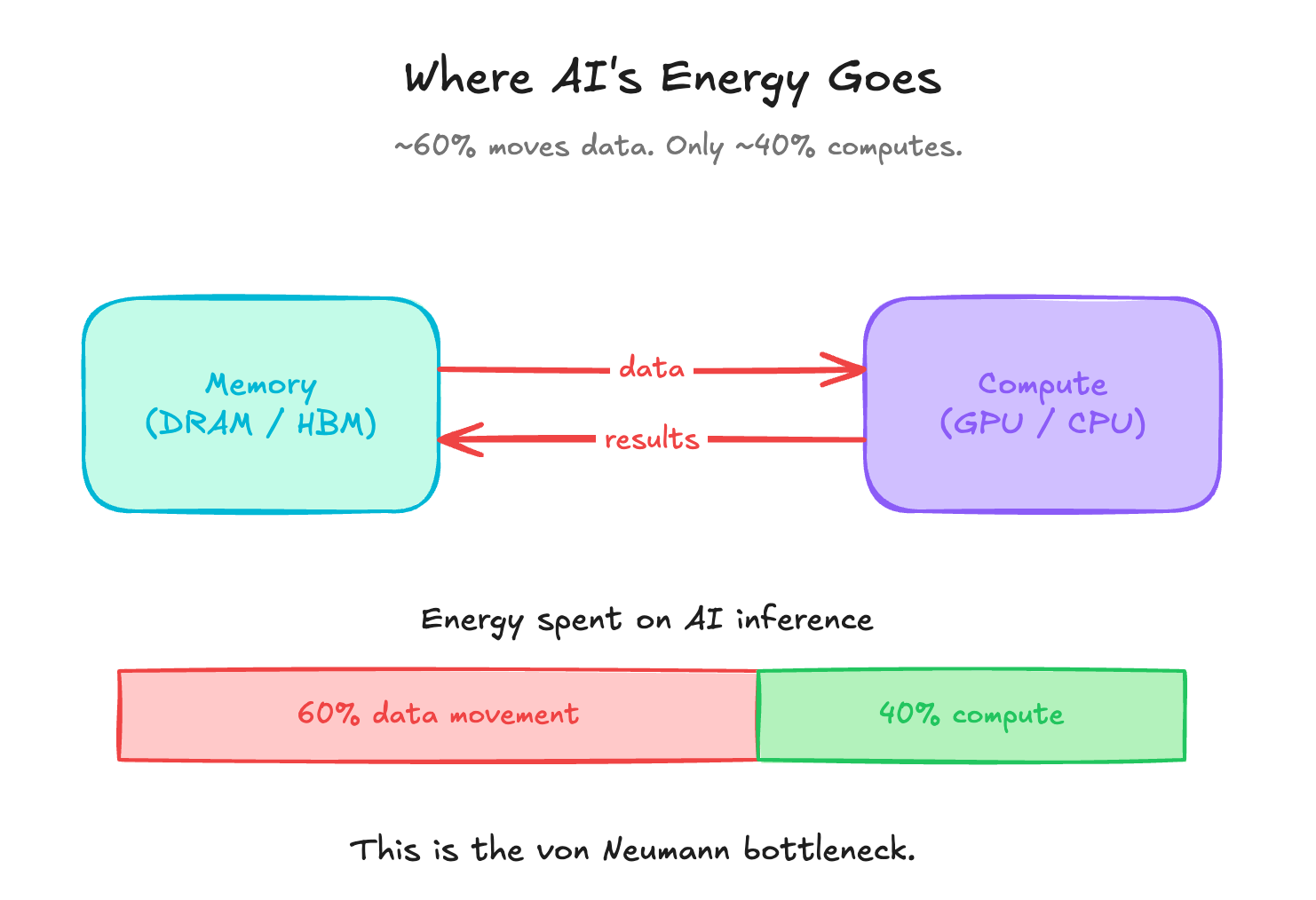
In modern AI workloads, about 60% of energy is consumed by data movement between memory and compute. Only 40% goes to the actual computation. The cause is structural. And incremental optimization on the current design will not shift the ratio.
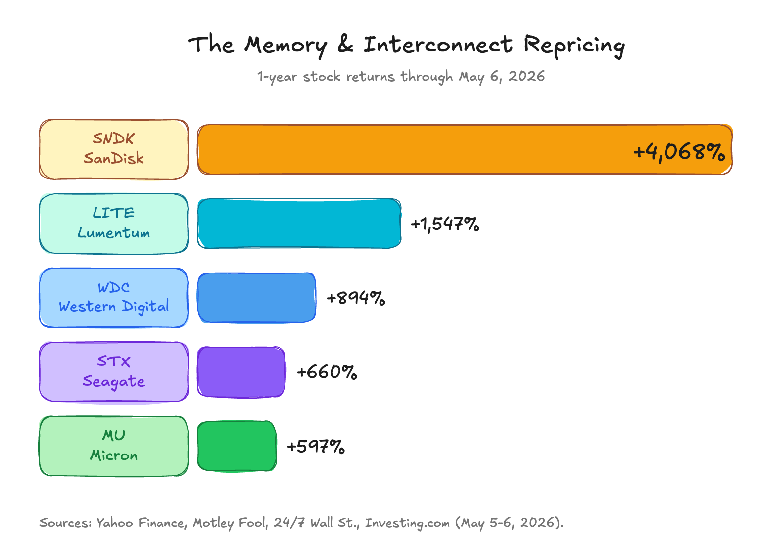
The public market has already noticed. The memory and interconnect layer is being repriced:
This post is an argument for why the next decade of silicon disruption will be decided in memory, and why the second-order effects of AI are reaching all the way down to the device layer of the stack.
How memory and compute actually work today
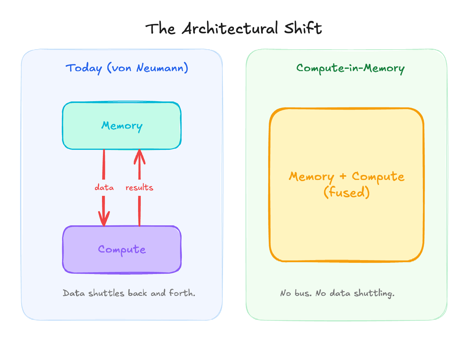
Every modern computer, including every AI accelerator, runs on an architecture sketched out by John von Neumann in 1945. Memory and compute are physically separate. Data lives in memory. Math happens in the compute unit. Every operation requires the data to travel: out of memory, across a bus, into the compute unit, and the result back again.
This worked beautifully for 50 years. It still works for most workloads. But AI breaks it.
Why? Because AI models are mostly weights: billions of numbers that have to be loaded and multiplied for every single token of output. A 70B model running inference is, mostly, a giant exercise in moving 70 billion numbers from memory to compute, multiplying them by inputs, and putting the results back.
Here’s the punchline: moving a number across a chip costs roughly 100 to 1000x more energy than the multiplication itself. So when your workload is dominated by data movement, as AI inference is, you’ve built a system where the bus, not the silicon, is the bottleneck.
This is what people mean by “the memory wall.”
Where the bottlenecks actually are
The “memory wall” gets used as a single phrase, but it’s really 3 different problems stacked on top of each other:
Bandwidth. Can you feed the GPU fast enough? This is what HBM (High Bandwidth Memory) was invented to solve. HBM4 is ramping in 2026. Turing Award winner David Patterson, the architect of RISC, recently called High Bandwidth Flash (HBF) the next bottleneck after HBM. SanDisk and SK Hynix are already collaborating on it.
Capacity. Can you fit the model? Industry sources are now reporting that CPU manufacturers are working to integrate 300 to 400GB of DRAM into AI CPUs, roughly 4x what a typical server CPU carries today. Models keep growing. Context windows keep growing. Agentic systems multiply both.
Energy. Can you afford to run it? This is the binding constraint. Data center power, not compute, has become the binding constraint Hyperscalers are now siting builds based on where they can find a few 100MWs of electricity. HBM is not just expensive: it’s brutally power-hungry, and a meaningful fraction of that power is going to data movement, not computation.
3 different bottlenecks. One root cause: memory and compute being physically separate.
What the incumbents are doing (and what they aren’t)
The legacy memory industry is dominated by:
SK Hynix (which holds roughly half the HBM market),
Samsung, and
Micron
SanDisk and Western Digital own the NAND flash side.
These are not sleeping incumbents.
Samsung has been shipping HBM-PIM (Processing-in-Memory) silicon.
SK Hynix has its AiM (Accelerator-in-Memory) product.
Micron is scaling HBM aggressively, and its CEO has recently been guiding investors toward dramatic upside in DRAM by 2028.
None of these companies missed the memory wall.
But here’s the structural problem: their P&Ls are anchored to selling more memory, faster. HBM is the highest-margin memory product in history. The economic incentive of the legacy memory business is to optimize the existing hierarchy, not replace it with a memory-compute fusion product that would cannibalize their best margin.
The most thoughtful read on Nvidia’s recent acquisition of Groq was that the value wasn’t in Groq’s compute, but in their SRAM design and the engineering around how memory feeds compute.
Compute-in-memory: the architectural turn
Here’s the alternative to the von Neumann split: stop moving the data. Do the math where the data already lives.
Compute-in-memory (CIM) is exactly what the name says. The multiply-accumulate operations that dominate every AI model (the same handful of arithmetic primitives, repeated trillions of times) happen inside the memory array. The weights never leave the memory cells. There is no bus to traverse. The energy cost of data movement, which dominates everything today, drops toward zero.
This isn’t a new idea. Researchers have been working on it for two decades. What’s changed is that the underlying device technology has finally crossed the threshold where production-grade CIM is achievable. New non-volatile memory devices can store multiple bits per cell, switch deterministically, and stack vertically into 3D arrays. The math finally works.
A few honest caveats. CIM almost certainly augments rather than replaces the existing memory hierarchy. The realistic outcome is a heterogeneous future where CIM handles inference at the edge and persistent weight storage near compute, while HBM and DRAM keep doing what they do for training and high-throughput cloud inference. The lesson from RISC vs. CISC is that the new architecture wins where it wins, but the old architecture rarely dies. The disruption shows up as a new layer in the stack rather than a replacement of the old one.
Why now
3 signals to take seriously.
Hyperscaler capex composition. When trillion-dollar buyers shift their composition (from GPUs to power to memory), secondary markets respond. The composition has shifted.
Public market repricing already underway. The chart at the top of this post tells the story. Every name on the chart is an industrial memory or interconnect business with real revenue and real customers. The repricing reflects real money concluding the constraint has moved.
Structural anchoring of the incumbents. They will optimize HBM. They will ship more PIM. They will not lead the architectural fusion that breaks their own margin structure.
The risk to flag: silicon timelines can be very long. Foundry partnerships, qualification cycles, and design-in to commercial silicon stretch over years. This is a long-cycle structural bet.
The silicon layer is due for disruption. AI’s second-order effects are reaching all the way down.
The bottleneck is not compute anymore.
60% of AI energy going to data movement not compute is the structural reframe. same memory wall pattern hitting our briefings this week from KV cache to HBM repricing